
Figure 1. The CADET.
Figure 1. The CADET.
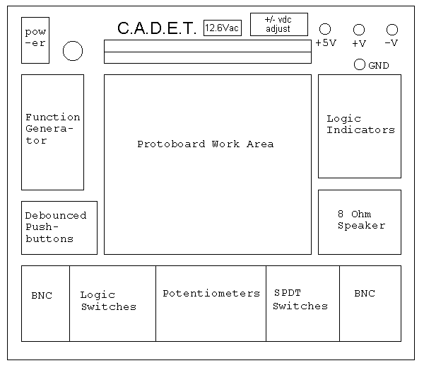
Figure 2. CADET Layout.
The C.A.D.E.T. analog/digital trainer (hereafter referred to simply as the CADET) shown in figure 1 provides the electrical energy for constructed circuits. Figure 2 shows the functional layout of the CADET. It has a +5 Volts dc source and 0 Volts (called ground and abbreviated GND). It also provides variable dc voltages between −15 and −1.3 Volts (labeled as −V) and +1.3 to +15 Volts (labeled as +V). The CADET has an on/off switch and a power indicator in the upper left corner.
The +5 V dc power supply can provide up to 1 ampere of current while the variable dc supplies can provide up to 500 mA, all with less than 5 mV of ac ripple.
A 12.6 Volt center-tapped ac supply is also available that can supply
up
to 100 mA.
CADET Function Generator
The function generator provides three waveforms (sine, triangular
and square wave) with a frequency ranging from 0.1 Hz to 100 kHz. The
amplitude of the
waveform is adjusted by the sliding control labeled AMP; the amplitude
varies
from 0 to 20 Volts peak-to-peak.
The TTL output is always a square wave and is not affected by the setting of the AMP control. The TTL output has rise and fall times that are 20 times faster than the regular square waves (25 ns vs. 0.5 µs).
CADET LoudspeakerThere is a switch to select between +5 V (TTL) mode and CMOS mode. The thresholds for TTL mode are 2.2 V for high and 0.8 V for low. In CMOS mode, the thresholds are 0.7*V and 0.3*V. The input impedance of the indicators is 100 Kohm.
The eight logic switches provide high and low signals. They are located in the lower left portion of the CADET. As with the indicators, there is a switch to select between +5 V (TTL) and variable levels.
When a switch's position is changed, it physically bounces before settling into its new position. This has undesirable results such as multiple occurrences of a digit on a calculator or of an extra character on a computer terminal. Some circuits you may construct are sensitive to this bouncing; in these cases debounced switches should be used. Some times there will be no need to be concerned with the bounce problem, then in those cases either kind of switch may be used.
Two debounced pushbutton switches are provided in the lower left
portion of the CADET. Each switch provides both a normally closed
(NC) and a normally open (NO) tie point to ground. Pushing the
switch causes the NC connection to open and the NO connection
to close. Releasing the switch causes the connections to return
to their normal state. The actual implementation of the outputs
of these switches is through the use of open collector output
devices. So to obtain a positive output voltage, it is necessary
to place a pull-up resistor between the output and Vcc. These outputs
can sink up to 250 mA.
The super strip provides a convenient means of constructing experimental circuits. The strip has two arrays of holes separated by a long (blank) channel, or gutter. Figure 3 illustrates a segment of such a strip. The holes are internally interconnected as shown. An integrated circuit chip is placed over the central channel so its pins make connection with the first column of holes on either side of the channel (for a small 0.3 inch IC). This leaves the four remaining holes in each row available to make connections to other points. The outer vertical "rails" (shown on the right in figure 3) are usually used to supply +voltage and ground to the circuit while the inner horizontal "rails" are used for signal connections.
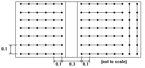
Figure 3. A Segment of a Super Strip.
These strips are appropriate for constructing experimental
circuits that involve low frequencies (up to a few MHz).
At higher frequencies, the large capacitance between the
adjacent rows of the connected holes can seriously
affect circuit operation.
To make connections to or between points on a proto board, use pieces of insulated solid wire of an appropriate diameter wire (good sizes usually are between #22 and #24 AWG). The insulation should be removed on both ends (leaving about three-eights of an inch of bare wire on the ends). Avoid twisting the end or bending it sharply such that it does not fit easily into the superstrip. Sharp bends anywhere in a wire can cause cracks to develop that may cause the wire to break under the insulation. To insert a connecting wire, push each end of the wire vertically all the way into a hole. A pair of long-nosed pliers are useful to help do this.
Before leaving the lab, check the floor and the benchtop for any stray pieces of wire.
It is very important to wire a circuit neatly. Such a circuit is less likely to contain errors, it is easier to debug, and it is easier to explain to the instructor or to a colleague.
The following suggestions should help you with your wiring of circuits.
The integrated circuits used in lab can look nearly the same. It is important to know how to tell them apart and how to locate pin 1. Each IC has a variety of information on its top which can include the manufacturer's name and location, a manufacturer's part number, and date of fabrication as well as the industry standard part number which is the item of primary interest to us.
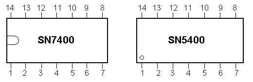
Figure 4. Two ways of identifying pin 1.
Figure 4 shows common ways of designating pin 1. Sometimes a notch is present, sometimes a dot, and sometimes both. In constructing circuits, wiring errors can be reduced and debugging aided by orienting the ICs in the same direction on the superstrip.
Be gentle in inserting and removing ICs from the superstrip.
Watch that pins do not get bent. Make sure that power and ground
connections are made to every IC and that they are made correctly.